USA, September 1, 2024 /EINPresswire.com/ -- Measuring computer chips to identify defects during manufacturing is crucial to improve production yield. Scientists from Delft and Utrecht investigated a novel imaging technique using EUV light—a high-energy short-wavelength radiation—to examine the 3D nanoscale structures on the chips. This technique eliminates the need to use any imaging system containing expensive EUV reflective mirrors in the measurement tool. Instead, images are reconstructed computationally from acquired diffraction data, resulting in a significant cost reduction.
Imaging plays a vital role in semiconductor manufacturing. Lithography scanners "image" the patterns on a template (mask) to the wafer to form functional structures such as transistors. The resolution of the imaging tools, i.e., the lithography scanners, determines the number of transistors per unit area. In principle, the higher the density of the transistors, the higher the computation power and energy efficiency.
According to Moore's law, this density should double every two years. As a result, the entire semiconductor industry is working on improving the resolution, and one important approach, based on the Rayleigh resolution criterion, is to decrease the source wavelength. This led to the invention of the latest EUV Lithography scanner by ASML—one of the most complicated machines humans have ever built. Using EUV lithography, the state-of-the-art 3nm technology node has achieved more than 200 million transistors per mm2.
Immediately following lithography, the structures formed on the wafer must be measured to identify defects. This is crucial to improve the production yield since defective chips can still be reworked by stripping the photo-resist layer on the wafer at this stage. Otherwise, such defective chips will continue to be processed through many unnecessary steps, causing an enormous waste of resources.
The measurement is usually another "imaging" process: the ultimate goal is to obtain an image of the sample. To match the resolution of lithography, the measurement should also use EUV light. However, such an imaging system will be so expensive that it will not be affordable in any semiconductor fab because its optical components, e.g., EUV reflective mirrors, are extremely challenging to fabricate at low cost.
One reason is that almost all materials absorb EUV light. So, only mirrors, not lenses, can be used, and to achieve sufficient reflection, either these mirrors must be coated with specially designed multilayer structures (acting as Bragg reflectors for EUV light) or, alternatively, EUV light must be incident on these mirrors at very small angles with respect to the surface (also known as the grazing incidence mirrors).
Besides, the overall aberration level of the imaging system must be smaller than a fraction of the EUV wavelength (e.g., 1/10 of the 13.5 nm EUV wavelength) to guarantee satisfactory image quality, and every mirror surface must be carefully polished to sub-nanometer precision to prevent scattering (a nuisance that further degrades image quality). Therefore, using any EUV imaging system in the measurement tool is economically not feasible.
In a recently published paper, scientists from Delft and Utrecht tried to solve this issue by investigating an alternative that does not rely on any imaging system but uses intensive computations. This approach is also referred to as "diffractive imaging" because the light reflected by the sample "diffracts" freely in space towards a camera. We reconstruct the sample image from the "diffraction pattern" acquired by a camera through a computationally intensive optimization process. We compare the two types of imaging methods in Fig. 1.
Now, we will introduce the key ingredients in this research:
The EUV source, the measurement scheme, and the reconstruction algorithm.
Compact Tabletop EUV Source
Traditionally, generating EUV light requires synchrotron radiation or free-electron laser sources in facilities as large as stadiums. However, a measurement tool must be reasonable in size to fit into a semiconductor fab. Therefore, we used a compact Tabletop EUV source in our experimental setup based on the high harmonic generation (HHG), of which the research area was awarded the Nobel Prize in Physics 2024.
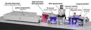
Fig. 2 illustrates our experimental setup. The compact tabletop EUV source consists of a pulsed infrared (IR) drive laser, a pulse compression unit, and a vacuum vessel for high-harmonic EUV generation. A picture of the HHG process is shown in Fig. 3, where the drive IR pulse laser is focused onto a pressurized Argon gas jet. A powerful pump maintains a high degree of vacuum (~10-5 Pa) in the vessel, while the pressure is much higher between the gas nozzle and the gas catcher. In this picture, we can observe the white plasma, which generates EUV radiation in the 10-20 nm wavelength range, and the scattered IR light in a purple-pink colour.
We shall note that compared to the source in ASML's EUV lithography scanner, which uses laser-produced plasma (LPP) to produce incoherent EUV light, the illumination produced by the HHG EUV source is directional and spatially moderately coherent—a property essential for reconstruction in diffractive imaging.
While the LLP sources in lithography scanners can generate ~250 W EUV radiation using a 20,000 W drive laser, the conversion rate of HHG sources is incredibly low: a 100 W drive laser only generates ~ 1 μW of EUV radiation (1011 EUV photons per second) at the gas jet, which is a 10-8 low conversion rate! Therefore, it is fair to say that every HHG EUV photon is precious.
Scanning Measurement Process
In our experimental setup, we focus the EUV beam onto the sample for illumination. The light reflected by the sample diffracts in free space, and we use an EUV camera to acquire the intensity distribution of the diffracted light, which is often referred to as the "far-field" diffraction pattern.
In the measurement process, we scan the focused EUV beam over the sample and acquire a diffraction pattern at each scanning position. This particular version of diffractive imaging is called "ptychography", which also requires enough overlap between the illuminated areas at neighbouring scanning positions. Unlike other scanning imaging techniques, such as scanning electron microscope (SEM) or atomic force microscope (AFM), ptychography reconstructs a 2-dimensional area rather than only a single pixel of the sample image at every scanning position.
Therefore, ptychography is significantly (several orders of magnitudes) faster than competing scanning imaging techniques because the reconstructed area per scanning position typically contains millions of pixels (for example, our EUV camera contains 2048 × 2048 ≈ 4 million pixels). The scanning mechanism also allows for infinite extension of the field of view, and the reconstructed sample image is free of stitching errors.
The redundant information due to the overlap of the sample's illuminated area allows us to use computational efforts to calibrate experimental uncertainties, such as those in the propagation distance and scanning positions (whose accuracy needs to be at the sub-nanometer level).
Powerful Algorithm
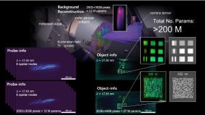
In this research, a powerful algorithm is required to reconstruct the sample image from the acquired scanning series of diffraction patterns. The reconstruction is done iteratively by "solving the inverse problem". While the forward problem is to build a model to simulate the process of ptychography based on model parameters, the related inverse problem is to retrieve model parameters from experimental data, which are the input and output pairs of the model, as illustrated in Fig. 4. To update model parameters, we also need a loss (error) function to compare the predicted and measured diffraction patterns and computing the gradient of the model parameters.
There are two main challenges: (1) the model can be very complicated, especially when considering multiple wavelengths and multiple spatial-modes for HHG EUV sources, and (2) the algorithm may require intensive computations.
For challenge (1), we use an automatic differentiation (AD) technology, which allows us to adopt a modular algorithm design. As we demonstrated in the paper, the model consists of concatenated sub-models presenting physical processes such as interaction, propagation, camera detection, etc. By guaranteeing each sub-model to be differentiable, AD can always compute the gradients of all model parameters. AD is superior to differentiation by hand derivation and finite difference because it can significantly reduce human efforts and numerical errors. AD also makes updates of model parameters a unified process instead of inventing "an update engine" for each model parameter. This leads to a drastic speed and memory improvement compared to state-of-the-art algorithms developed using conventional approaches.
The remedy for challenge (2) is to use GPU acceleration at every step of the algorithm. This leads to an enormous speed improvement. Especially the fast Fourier transform (FFT), which is essential to compute the propagation from the sample to the camera, can be accelerated by a few orders of magnitude by using GPU.
Both AD and GPU acceleration are now implemented in standard machine-learning platforms such as Tensorflow (used in this work), PyTorch, etc. These technologies, which enable the training of artificial intelligence (AI) models and thus power AI's prosperity, now also power the optimization in our ptychography algorithm, enabling us to calibrate experimental uncertainties, handle spatial coherence degradation, and perform wavelength-multiplexed reconstruction.
Building the future tool to measure computer chips for defect identification during manufacturing is an endeavour that requires an advanced short-wavelength compact light source (HHG EUV source), a novel imaging method (diffractive imaging: ptychography), and a powerful reconstruction algorithm using technologies that enable AI training and benefit from the explosive growth of AI.
DOI
10.1038/s41377-024-01558-3
Original Source URL
https://doi.org/10.1038/s41377-024-01558-3
Funding information
This publication is part of the project "Lensless Imaging of 3D Nanostructures with Soft X-Rays (LINX)" with project number P16-08 of the Perspectief research programme financed by the Dutch Research Council (NWO).
Lucy Wang
BioDesign Research
email us here
Legal Disclaimer:
EIN Presswire provides this news content "as is" without warranty of any kind. We do not accept any responsibility or liability for the accuracy, content, images, videos, licenses, completeness, legality, or reliability of the information contained in this article. If you have any complaints or copyright issues related to this article, kindly contact the author above.
© 2025 Benzinga.com. Benzinga does not provide investment advice. All rights reserved.
Trade confidently with insights and alerts from analyst ratings, free reports and breaking news that affects the stocks you care about.


